Significant Progress Made by Wu Xu’s Research Group in Building Strong Interlayer Coupled Two-Dimensional Semiconductor Heterostructures
Date:02-26-2025
The research group led by Professor Wu Xu from the School of Physics and the Academy for Advanced Interdisciplinary Studies at Beijing Institute of Technology has achieved a significant breakthrough in the field of transition metal dichalcogenide (TMD) heterojunctions. This research finding, titled “In-Plane Transition Metal Dichalcogenide Junction with Nearly-Zero Interfacial Band Offset,” has been published in the internationally renowned journal ACS Nano (ACS Nano, 19, 1, 803-810, 2025, DOI: https://doi.org/10.1021/acsnano.4c12092).
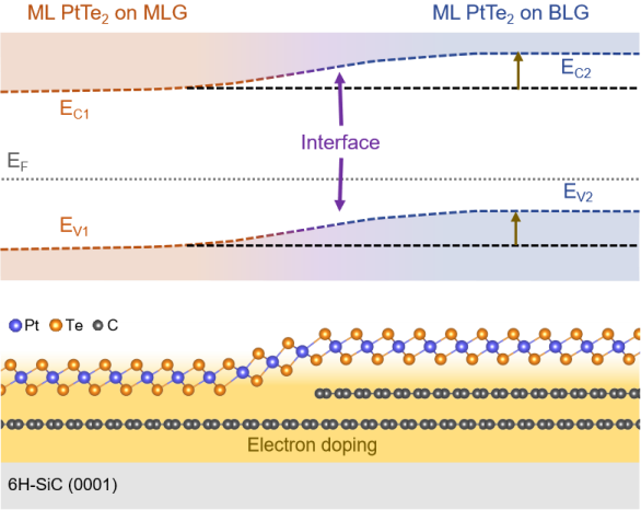
Two-dimensional in-plane transition-metal dichalcogenide (TMD) junctions have a range of potential applications in next-generation electronic devices. However, limited by the difficulties in ion implantation on 2D systems, the fabrication of the in-plane TMD junctions still relies on the lateral epitaxy of different materials, which always induces lattice mismatch and interfacial scattering. Here, we report the in-plane TMD junction formed with monolayer (ML) PtTe2 at the boundary of ML and bilayer graphene on SiC. As the scanning tunneling microscopy/spectroscopy results revealed, the substrate screen effect is weak on ML PtTe2, compared to the nonlayered materials. At the interface of the junction, the atomic lattice is continuous, and a smooth type-II band alignment is formed with a near-zero band offset. The reported technique can be readily extended to other 2D semiconductors with strong interlayer coupling and is feasible for fabricating TMD junctions with promising interfacial electronic structures, aimed at device applications based on low-dimensional electronic behaviors.
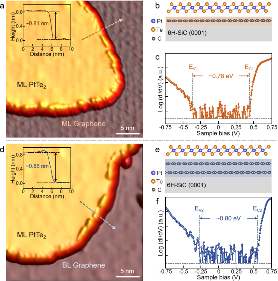
Fig.1 STM Images of Monolayer PtTe2 Islands on Monolayer/Bilayer Graphene.
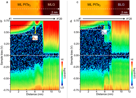
Fig.2 Energy Band Bending of Monolayer PtTe2 Edges on Monolayer/Bilayer Graphene.
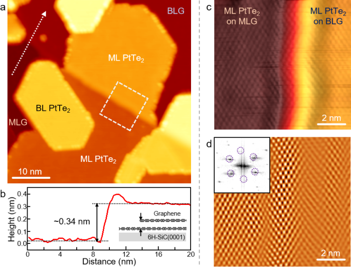
Fig.3 PtTe2 Islands Across the Monolayer/Bilayer Graphene Boundary Exhibit a Continuous Atomic Structure.
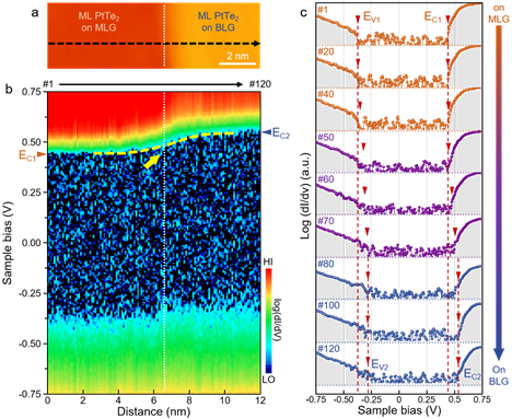
Fig.4 Band Alignment of Monolayer PtTe2 at the Monolayer/Bilayer Graphene Boundary, Showing Significant Energy Level Variation.
Fig.5 Schematic Diagram of Substrate Charge Transfer Screening by Monolayer/Bilayer Graphene